

AI Chip Design Hits Crossroads in Agentic Era
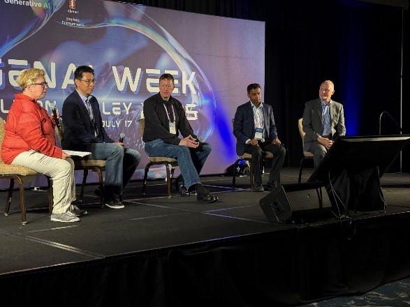
As AI continues its meteoric rise, the technologies enabling that growth – compute, memory, networking, and chip architecture – are being stretched to their limits. While the pace of innovation is accelerating to address these limits, the application of AI in the workflows continues to innovate as we move from reinforcement learning to generative AI and now, AgenticAI. During Gen AI Week, I had the distinct honor of moderating a panel of silicon industry heavyweights to explore how the next wave of chip design is evolving to meet the challenges of large-scale AI deployment.
Our discussion underscored a common theme: the age of agentic AI is upon us and it will fundamentally reshape how chips are architected, manufactured, and even conceived.
Joining me on stage were:
- Harish Bharadwaj, VP of marketing in the ASIC product division at Broadcom
- Bob Brennan, VP of customer solutions engineering at Intel Foundry
- Kelvin Low, VP of sales at Samsung Foundry
- John Koeter, SVP at Synopsys, leading IP development
Why AI Is Reshaping Semiconductor Design
The panel kicked off with a look at the current state of chip design and why AI is creating unprecedented pressure on silicon teams. As AI models double in size nearly every year, chipmakers must accelerate the speed and the intelligence of their design processes.
Kelvin Low of Samsung Foundry pointed to the growing complexity of IP subsystems, which are now often pre-optimized for AI workloads. He noted that the industry is moving beyond traditional chipmaking, focusing instead on delivering pre-optimized IP subsystems and full-stack solutions tailored to specific AI workloads.
John Koeter echoed that sentiment, highlighting how today’s hyperscalers are pushing for 5–10x improvements in silicon performance, at a time when Moore’s Law and Dennard scaling are plateauing. He emphasized that the semiconductor industry is at an inflection point, where traditional scaling is no longer enough and entirely new approaches, like multi-die design and agentic AI, are needed. We need to re-engineer design workflows from the ground up.
Compute, Memory, and the Architecture Bottleneck
While GPUs have dominated headlines, the panelists emphasized that AI infrastructure relies on a broader constellation of compute and memory technologies. Brennan outlined two parallel trends: going big with monolithic training chips and going out by scaling across multiple smaller units.
He also introduced the idea of compute density versus capacity, especially when it comes to high-bandwidth memory (HBM). He stressed that while HBM plays a key role in performance, it also introduces significant power challenges – accessing these memory stacks alone can consume hundreds of watts.
Low explained how the industry is working on custom HBM stacks optimized for specific workloads, with next-gen configurations offering lower power and higher integration thanks to basedies utilizing a logic-process instead of a DRAM process.
“Power is everything,” he said. “We just do not have enough power to fit into the data center. So wherever possible to reduce power, we can do that.”
Data Movement and Networking: From Bottleneck to Co-Architect
As AI clusters grow from 20,000 to 100,000+ compute nodes, network infrastructure is becoming a primary design constraint.
Harish Bharadwaj explained that AI workloads are pushing data movement beyond traditional thresholds. He noted that AI cluster-level bandwidth is growing up to 10x in a single year, driving the need for far more scalable and efficient network infrastructure.
John Koeter added that networking is no longer just a back-end concern; it has become a critical co-architect of overall system performance. Koeter expanded on the evolution of standards.
“The time between standards used to be three to four years, and that’s been accelerating to 2 years to 18 months,” he said. “And the question is, ‘Why?’ And that’s across the board – memory interface, PCI Express...even good old USB. The interface standards are accelerating. And the reason is because you can pack an enormous amount of compute units onto a chip, but you have to be able to transfer data on and off that chip very, very efficiently.”
Enter Agentic AI: Reinventing the Engineering Workflow
One of the most exciting – and existential – topics of the panel was the rise of agentic AI, or the use of autonomous software agents in chip design workflows.
Koeter explained that AI is transforming not just what engineers design, but how they design. He described a future where networks of autonomous agents assist with key stages of chip development – prompting teams to completely rethink and rebuild traditional engineering workflows from the ground up.
From macro placement to RTL generation, panelists said agentic AI is beginning to automate and optimize historically manual tasks. Brennan noted that although silicon engineering lacks the vast open-source data available in software, AI tools are already producing meaningful speedups.
“What used to take weeks now takes hours,” Bharadwaj said.
Still, the panelists agreed: AI won’t replace chip designers, but designers who use AI will replace those who don’t.
Workforce Implications: New Roles, New Challenges
Agentic AI is also reshaping how teams are structured and trained.
Brennan pointed to workforce challenges, citing predictions that the industry could be short a million engineers in agentic AI by 2030.
“The cool kids are no longer going into silicon,” he said. “They’re going into algorithms and software.”
The panelists called for a shift in training and team structure, with junior engineers gaining AI-augmented capabilities once reserved for veterans. But challenges remain – particularly around proprietary data security and best practices that haven’t caught up with the tech.
Measuring the Payoff
When asked how teams are quantifying productivity gains, Bharadwaj was clear: it’s about pace. He noted that companies are under intense pressure to launch new xPUs annually, and that technologies like agentic computing may play a crucial role in helping the industry keep pace.
Koeter offered a final perspective.
“I tell my team all the time… there’s two types of design engineers in the future: ones that lean in and embrace agentic AI with all their hearts, and dodos and dinosaurs,” he said. “I’m like, don’t be a dodo. You gotta lean in.”
The TechArena Take:
AI is no longer just a workload. It’s a force reshaping the silicon landscape. From custom memory to co-architected networks, and agentic workflows to workforce transformation, this panel revealed the full-stack rethink underway as the industry races toward a trillion-dollar AI economy.


.png)


